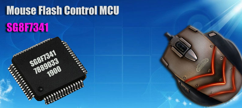
SG8F7341
General Description:
SG8F7341, is a can be used for gaming mouse control chip, and low power consumption and high-performance 8051 structural microcontroller of other equipment development. There is Power-on Reset, LDO, clock oscillator, watchdog, timer, high accuracy PWM on chip and ADC. Then have integrated I2C and UART standard communication protocol port on chip. FLASH of chip in system have program ability again, be used for nonvolatile data storage, and allow the IAP (In Application Programming).
Features:
- Speed of 8-bit high-performance MCU up to 48 MHz
- 16 KB FLASH program memory
- Support debug and program and burn the USB port online
- 256 byte internal common RAM and 512 byte extend XRAM
- Support the UART, the I2C port
- Support DMA communication
- Built-in high-precision PWM
- Internal integration 12-bit high resolution ADC
Clock System
- High-speed programmable RC (12 MHz) on chip
- PLL 48M on chip
- Low speed RC (500 KHz) on chip
- Support spread spectrum clock generator (SSCG)
- Without external crystals under FULL SPEED USB application, built-in USB clock recovery circuit
GPIO
- General bidirectional input/output port (Optional voltage 5V or 3.3V)
- With a built-in pull-up resistor
- Can realize open drain output
- Adjustable output driving capability (4mA/20mA two optional irrigation current gear)
USB Controller
- Compatible with USB 2.0 support at full speed and low speed two modes
- Supports 3 endpoints
- Support DMA transfers
- The data depth of endpoint 0 is 8 byte
- The data depth of endpoint 1 and endpoint 2 is 64 byte
I2C Port
- Can be used as host or slave
- Support the I2C STAND/FAST mode
- Slave mode compatible with 8/10 address
PWM0/1/2
- Complementary output and control dead zone time
- High-precision PWM regulating function
- When the system clock choosing low frequency, PWM still working in high frequency
ADC
- Accuracy is 12 bit
- Maximum 250 ksps
- Four file optional reference voltage, respectively VDD5, VDD3O, external or internal 2.0V
FLASH Memory
- Can realize the IAP in specific regions
- Capacity of 16 KB
- Each page 256 byte
- Program the FLASH by the USB port (need programming device to support)
Power System
- Built-in 5V to 3.3V LDO
- Built-in 5V to 1.8V LDO (digital system supply power)
- Support two kinds of low power mode (IDLE/STOP)
Debugging Port
- Debugging port at full speed, non-invasive in system (on chip)
- Single-step debug
- Can read or modify the internal memory and registers
UART Port
- You can choose whether to bring the parity bit
- Baud rate can be adjusted
Timer/Counter 0/1
- Compatible with Timer 0/Timer 1 of MCS-51
- Optional timer clock
- Four kinds of working mode
Timer 2
- Timer 2
WDT
- Can be used as a reset/wake up the source